Printed electronics and SMD (surface mounted device) technology - the best of both worlds


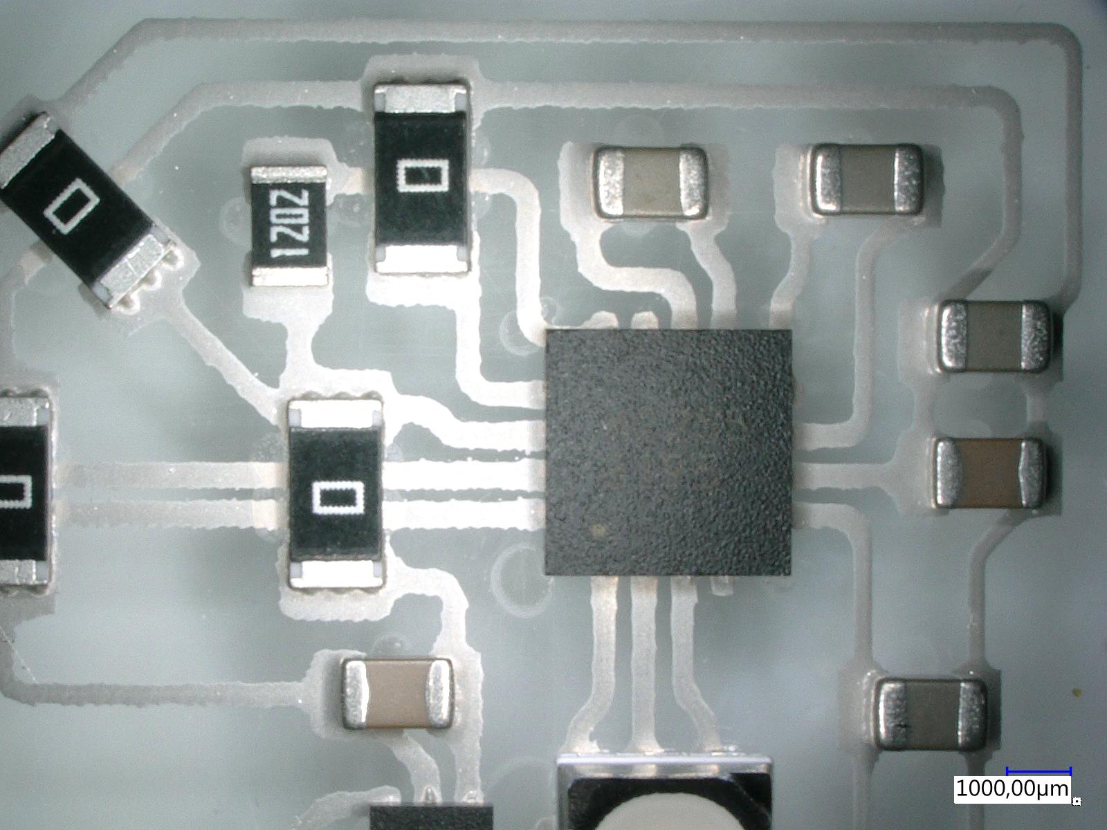
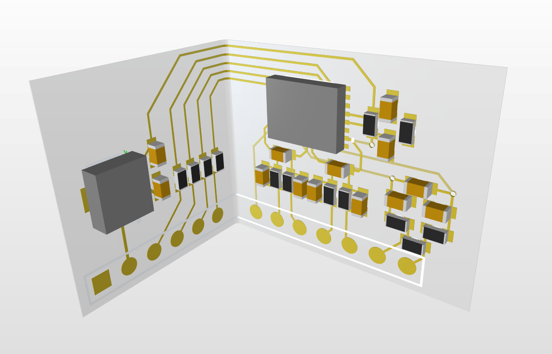
The combination of printed electronics and SMD components opens up new design possibilities and integration options into products. Multilayer circuits can be printed layer by layer on a flexible film and then assembled. This technology not only offers great potential for lightweight construction, but is also an environmentally friendly alternative to the conventional multilayer PCB (printed circuit board) due to the absence of glass fibre composites.
How the technology works
The circuit design is created analogue to the classic PCB. Screens are then produced for each conductive and insulation layer. Conductive and insulation layers are now printed alternately onto a substrate, whereby vias, i.e. electrical connections, can be integrated in the Z direction. The top layer contains the contact pads for all SMD components. This is followed by the application of electrically conductive and non-conductive adhesive dots and then the automatic placement of the SMD components using a pick and place process. A top coating is applied to embed the components and protect them from moisture. The overall structure is very similar to a classic PCB, but offers several advantages.
The advantages of printed PCBs
Production can be implemented on site with a low investment in equipment, allowing dynamic in-house production to be set up. Compared to conventional PCBs, the printed version is lighter and enables a lower construction height. In addition, no glass fiber reinforced plastic (GRP) is used, but thin thermoplastic films can be used, making this screen-printed version significantly more sustainable.
Functionalization is a core competence of Fraunhofer IFAM. Jonas Deitschun's "Functional Printing" working group researches and develops functionally integrated components and surfaces. In the "Advanced Printing Technologies" department, the group has extensive know-how and the latest technologies with a focus on ink and paste development as well as printed electronics and sensor technology. The fields of application range from automotive engineering and aircraft manufacturing to energy and medical technology.
 Fraunhofer Institute for Manufacturing Technology and Advanced Materials IFAM